VIGO PHOTONICS · SMART TAIWAN
VIGO III-V epitaxial wafers and photonic structures
Epi-Wafers
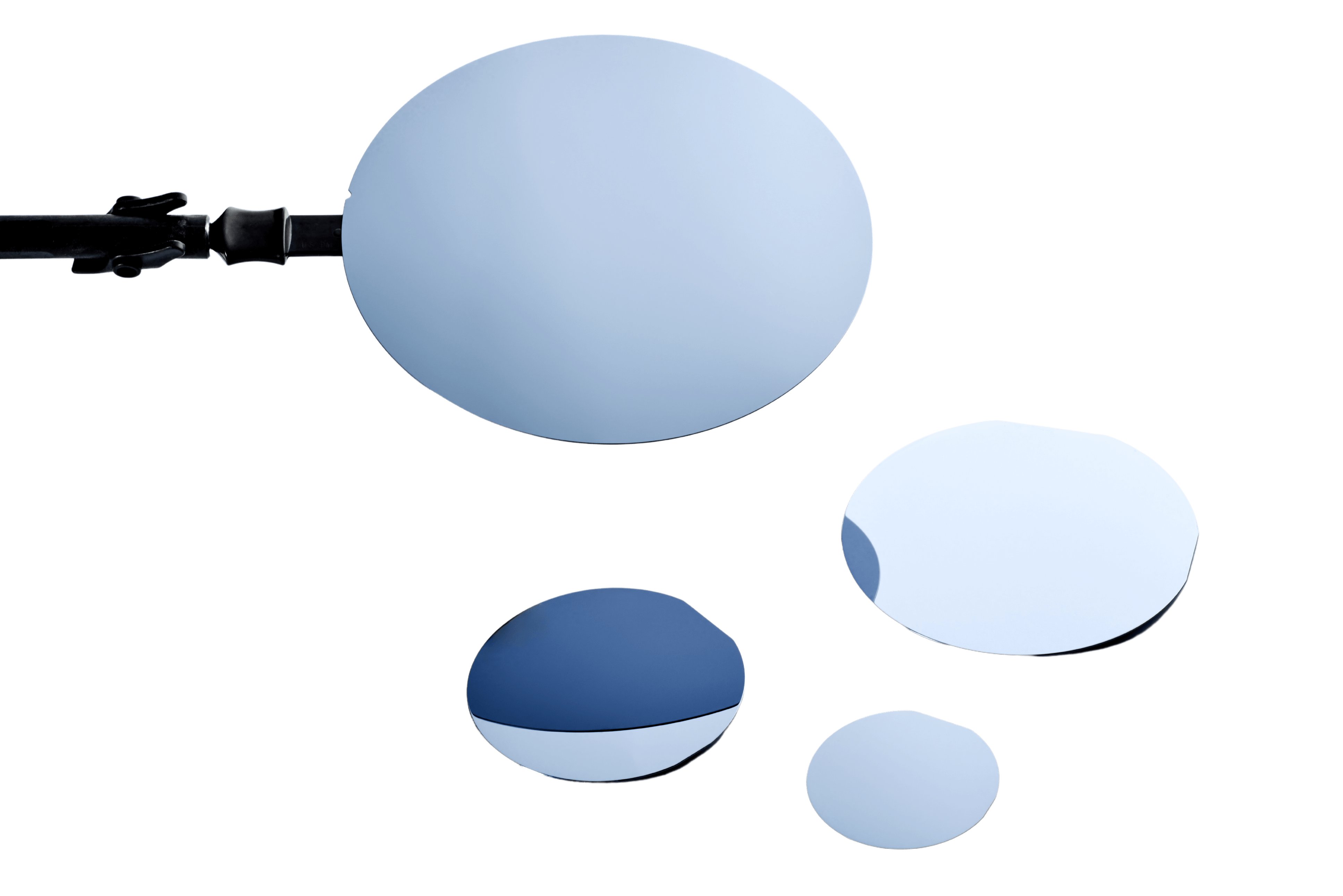
Evaluate GaAs- and InP-based III-V epitaxial structures for photonic-device development. SMART coordinates substrate, layer-stack and characterisation requirements with VIGO for InGaAs photodetector, VCSEL or QCL projects.
Specifications and configuration
| Substrate / material platforms | GaAs-based and InP-based III-V structures |
|---|---|
| Photodetector structures | InGaAs PD epi-structures |
| Laser structures | VCSEL / QCL / edge-emitting laser structures |
| Supply basis | Custom structure and project quotation |
| Initial inputs | Target device, substrate, stack, dimensions, characterisation and volume |
Custom structures: specifications, tolerances and acceptance criteria are agreed per project.
Typical values are not guaranteed limits. Refer to the original English datasheet for full test conditions, minimum / maximum values and operating limits. D* figures measured at different frequencies are not directly comparable.
Selection and integration considerations
- Provide the layer stack, doping, substrate, target wavelength, wafer dimensions and characterisation methods, or begin with the intended device.
- Epi-wafers are process inputs, not packaged lasers, detectors or ready-to-use modules.
- Pilot batches and production schedules depend on structure feasibility and agreed acceptance requirements.
Original English documents and resources
Start with your measurement requirements
Share the model or application, wavelength, signal bandwidth, quantity and desired schedule. Unknown items can be discussed during selection.
Submit a VIGO inquiry